You’ve got your boards assembled. Now how do you know they actually work?
Testing. But not all testing is the same. Here are three common methods – and which one you need.
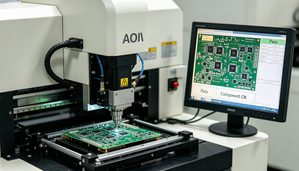
1. AOI – Automated Optical InspectionAOI
How it works: Cameras take high‑resolution photos of your board and compare them to a perfect image. It catches missing parts, wrong polarity, and bad solder joints.
Good for: Fast, non‑contact checking. Works on most surface‑mount components.
Limitations: Can’t see under BGAs or inside solder joints. Won’t catch a dead chip.
When to use: Always – even for prototypes. It’s cheap and catches obvious mistakes.
2. ICT – In‑Circuit Test
How it works: A bed‑of‑nails fixture touches test points on your board. It measures resistors, capacitors, shorts, and opens. It can even power up individual circuits.
Good for: Very reliable. Finds manufacturing defects like a missing capacitor or a shorted trace.
Limitations: Requires a custom fixture ($300‑$1,000) and test points on your PCB. Slower to set up.
When to use: Medium to large production runs (100+ boards). Essential for medical, automotive, or any high‑reliability product.
3. FCT – Functional Test
How it works: You power up the board and run real firmware. Push buttons, check LEDs, read sensors, measure outputs. It tests if the board does what it’s supposed to do.
Good for: The only test that proves the board works in real life.
Limitations: You need to write the test procedure and maybe build a simple fixture. Labour‑intensive.
When to use: Every board should get at least a basic functional test. For prototypes, do it yourself. For production, ask your CM to run it.
Everyone wants to save money on PCBA. But cutting corners on quality isn’t the answer. Here are eight real ways to lower costs without breaking your board.
Reduce Unique Component Values Do you really need 10 different resistor values? Each unique part adds handling time and inventory cost.
Do this: Use standard values (10k, 1k, 100nF) across your design. Merge similar values where possible.
Choose Standard PCB Thickness 1.6mm is the most common board thickness. It’s cheap and widely available. Going thinner (0.8mm) or thicker (2.0mm) often adds cost.
Do this: Stick to 1.6mm unless you have a good reason not to.
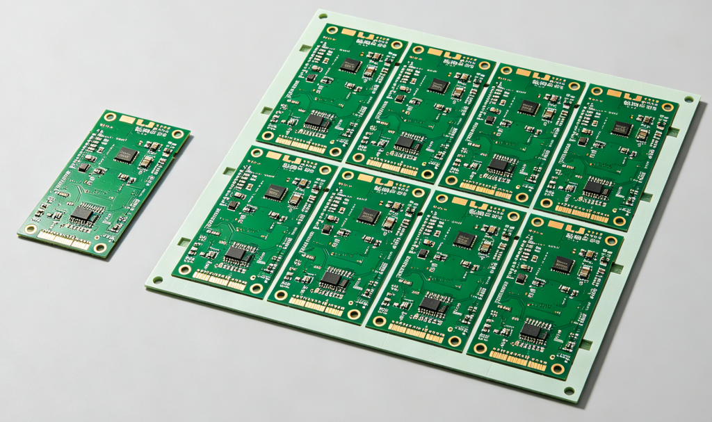
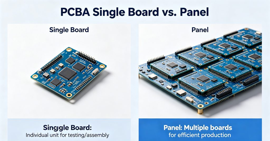
Panelize Your Boards Running single boards is slow. Panelizing (putting multiple copies on one large board) saves machine time and reduces per‑board cost.
Do this: Ask your CM for panelization recommendations. Keep components away from edges.
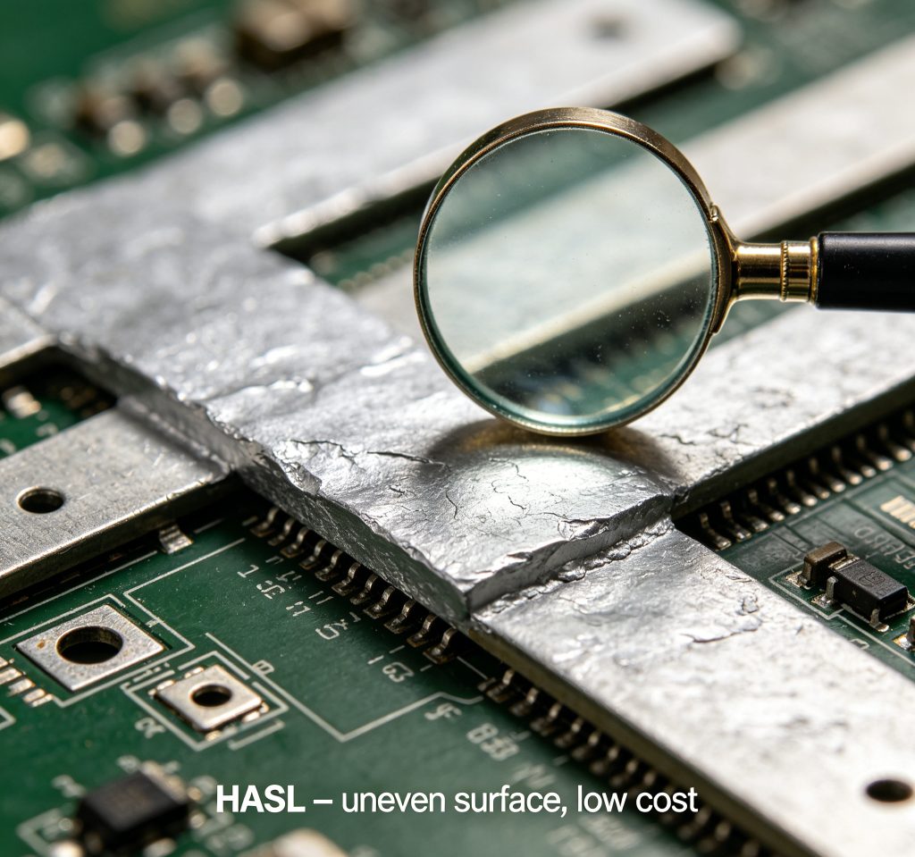
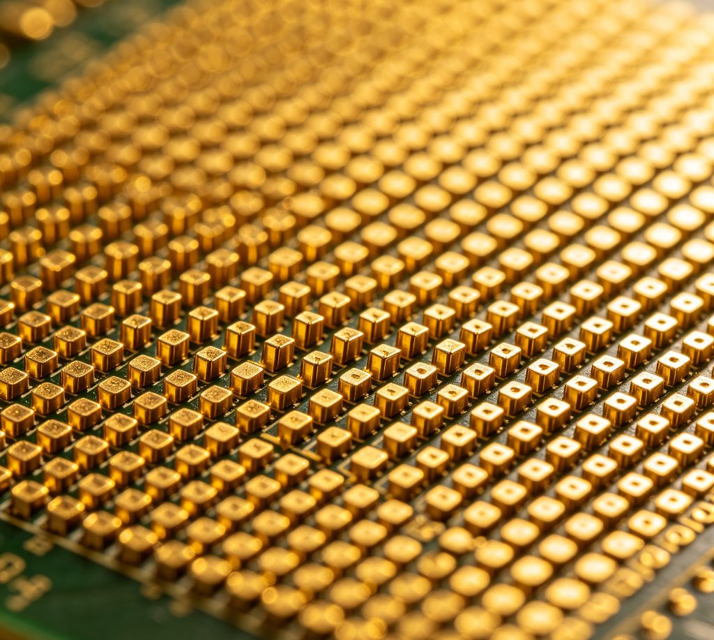
Use HASL Instead of ENIG If Possible ENIG looks nice and works great for fine‑pitch parts. But it costs 2–3x more than HASL.
Do this: Use HASL for simple boards and prototypes. Save ENIG for BGAs or gold fingers.
Order Components in Bulk Buying 100 resistors as cut tape costs more per piece than buying a full reel of 5,000.
Do this: Plan ahead. If you know you’ll run more boards later, order extra parts now.
Avoid Exotic or Obsolete Parts A $0.50 part that’s end‑of‑life can cost $5.00 from a specialty distributor – if you can find it at all.
Do this: Check component availability before finalizing your BOM. Use active, common parts.
Combine Multiple Designs into One Order If you have two small boards, consider running them together on the same panel. Setup fees get shared.
Do this: Ask your CM if they can panel different designs together. Many can.
Get a DFM Review Before You Order Catching a design mistake early costs nothing. Catching it after production costs time and money.
Do this: Always request a free DFM report. Fix the issues before you commit to a large run.
The Bottom Line Lower PCBA cost isn’t about finding the cheapest factory. It’s about smarter design, smarter BOM, and better planning. Start with these eight tips, and you’ll see real savings.
Over the years, customers have asked me the same questions again and again. So here they are – short, honest answers. No sales pitch.
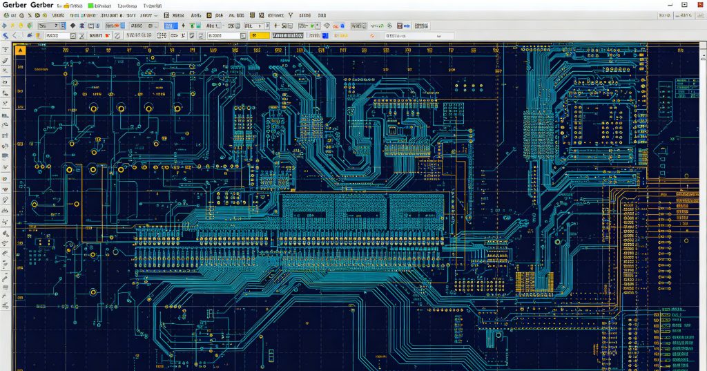
What files do you need to start? Gerber files (for the PCB), BOM (component list), and centroid file (where parts go). That’s it. Missing any of these and we can’t start.
What’s your minimum order quantity (MOQ)? For PCBA, no minimum. I’ve done 5 boards for a prototype. But keep in mind: small batches have higher per‑board cost because setup fees don’t change.
Can you source components for me? Yes. Most customers prefer that because we get better prices and catch obsolete parts early. You can also send your own parts – just let us know upfront.
Do you provide a DFM report? Yes, and you should never skip this. We run your files through DFM software before production. It catches things like missing thermal reliefs or pads too close together. Free of charge.
How long does PCBA take? Typical lead time: 5–10 working days after all components arrive. Add 2–3 weeks if parts need to be ordered. Rush service is possible but costs extra.
Do you test every board? For prototypes, we do visual inspection and basic functional test if you provide instructions. For production runs, we recommend AOI or ICT on 100% of boards. Skipping testing saves money but risks returns.
What if some boards fail testing? We rework them at no extra cost if the failure is our fault (wrong component, bad solder joint). If it’s a design issue or bad part you supplied, we’ll tell you and charge for rework.
Your prototype worked. Now you want 1,000 boards. Same design, right? Not exactly.
Here’s what changes when you scale.
Panelization For 10 boards, they run singles. For 1,000, they panelize – multiple boards on one large sheet. Saves cost, but adds depaneling. Keep components away from edges.
Machines Change Prototypes use slow, flexible machines. Mass production uses high‑speed chip shooters. Those need clean fiducials and uniform part heights. Design for speed.
Component Sourcing Small volumes = cut tape. Large volumes = full reels. Some parts that were available for prototypes may be backordered for reels. Check availability early.
Testing Scales Visual inspection works for 10 boards. Not for 1,000. You’ll need AOI, ICT, or functional test fixtures. Budget for them.
Lead Times Prototype: 5‑7 days. Mass production: 3‑4 weeks. Everything is batched. Plan ahead.
Per‑Board Price Drops, But Setup Costs Rise Yes, each board gets cheaper. But you pay for panelization, test fixtures, programming – often 500 – 500–2,000 upfront. Spread across 1,000 boards it’s fine. For 200 boards, it hurts.
The Takeaway Don’t assume production works like prototyping. Talk to your CM early. Plan for panelization, testing, and longer lead times. Scale smart, not hard.
You get three quotes. You pick the cheapest. Then the boards arrive late, or they don’t work, or the factory ghosts you.
I’ve been there. Here’s what I wish I knew before choosing a PCBA supplier.
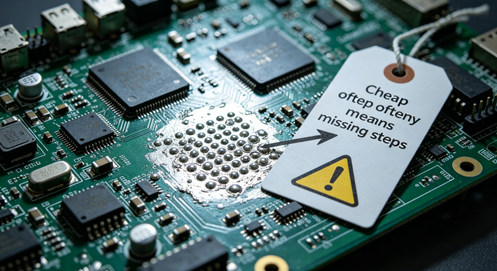
The cheapest quote is a trap A low price usually means skipped steps – no solder paste inspection, no cleaning, minimal testing. You’ll pay for it in rework later.
Do this: Ask what’s included. If they can’t tell you, move on.
Test their communication first How they reply before the order is how they’ll reply when something goes wrong.
Do this: Send a technical question. If they take 3 days to answer, imagine how long they’ll take when your boards are delayed.
Ask where they buy components Fake parts ruin boards. Some factories buy from whoever is cheapest.
Do this: Ask “Do you use authorized distributors?” If they hesitate, be careful.
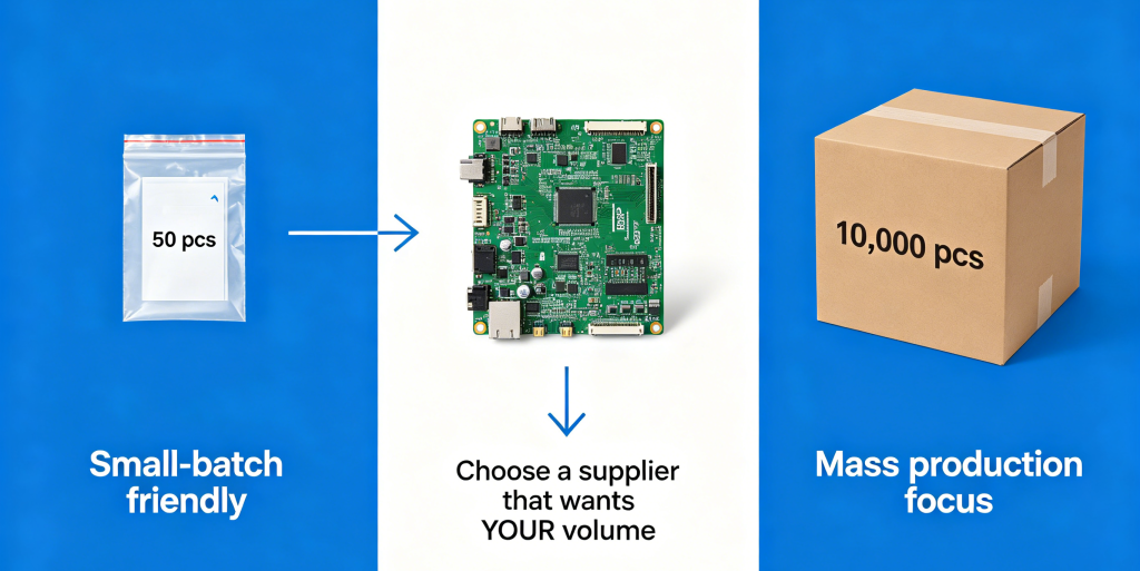
Know if they do small batches Some factories only want 10,000 boards. They’ll quote you a crazy price for 100 because they don’t want the job.
Do this: Ask their typical order quantity. Find a shop that actually likes small runs.
Get a DFM review Design for Manufacturing catches problems before they cost you money.
Do this: Ask “Do you offer a free DFM report?” If no, find someone who does.
Don’t assume testing Visual inspection isn’t enough for serious products.
Do this: Ask exactly what tests they run. AOI? ICT? Functional test? Get it in writing.
Judge them on the second order Anyone can look good for one small batch. The real test is the second order.
Do this: Place a small test order first. Then a second. If quality drops, you know.
Red flags to walk away from: Price is half of everyone else’s
You get a quote. It’s 3,000for100boards.That’s30 each. But the parts on DigiKey only cost 8.Sowheredidtheother22 go?
I’ve seen this confusion a hundred times. People think PCBA pricing is a mystery. It’s not. It’s just a stack of costs, and most of them aren’t obvious.
Here’s what you’re actually paying for.
The Short Version
A PCBA quote usually breaks down like this:
Components – 40–70% of total cost
PCB bare board – 10–25%
Assembly (setup + placement + soldering) – 15–30%
Testing – 5–15%
Extras (stencil, programming, coating, shipping) – the rest
Now let me walk you through each piece.
1. Components – The Big One
This is where most of your money goes. Resistors, capacitors, connectors, ICs, LEDs – they add up fast.
Why it’s expensive
Some chips cost $10 each by themselves
Minimum order quantities (MOQs) – you might need 1000 pieces when you only want 50
Supply chain issues – a 0.50partbecomes5 if it’s out of stock
Brand vs. generic – original parts are safer, but cheaper alternatives exist
How to save Let your CM source parts. They have relationships with distributors and can find alternatives you didn’t know existed. Just don’t go too cheap – fake parts are real.
Real example A Bluetooth chip I used last year: 4.20fromMouser.MyCMfoundagenuinebatchfor2.80 because they bought 5000 at once and shared with another customer. Saved me $1.40 per board.
2. PCB Bare Board – Not Just a Slab of Green
The empty board itself costs money. How much depends on:
Layer count – 2 layers is cheap. 6 layers is not.
Material – standard FR4 is fine. High‑TG, Rogers, or aluminum? Price goes up.
Surface finish – HASL (cheap), ENIG (gold – more expensive but better for fine‑pitch parts).
Hole size & density – lots of small vias add cost.
Rule of thumb A typical 2‑layer, 100x100mm board in small quantity (50–100 pieces) might cost 2–5each.A6‑layerboardcouldbe15–30.
3. Assembly – The Part Nobody Thinks About
You have the PCB. You have the components. Now someone has to put them together.
Assembly cost includes:
Stencil – a one‑time fee ($50–150) for the metal sheet used to apply solder paste
Programming – loading your pick‑and‑place file into the machine ($50–200, often waived for small runs)
Placement – per‑component cost. Typical: $0.01–0.05 per resistor/capacitor, more for large ICs or connectors
Soldering – reflow and wave soldering time
Labor – manual insertion for through‑hole parts (connectors, big capacitors)
Why small batches hurt The setup cost is almost the same for 10 boards as for 1000. So your per‑board price is high at low quantities. That’s why 5 boards might cost 20each,but500boardscost8 each.
Real example A customer wanted 20 boards assembled. Setup + stencil + programming was 300.Componentswere200. PCB was 40.Total540, or 27perboard.Heaskedfor200boardsnexttime.Totalwas1800, or $9 per board. Same design. Half the per‑board cost.
4. Testing – Cheap Insurance or Expensive Mistake
Testing adds cost. Skipping testing adds risk.
AOI (automated optical inspection) – cheap, often included. Cameras check for missing parts and obvious bridges.
ICT (in‑circuit test) – a custom fixture touches test points. Reliable but costs $200–1000 for the fixture. Worth it for medium to large runs.
FCT (functional test) – you or the factory powers up the board and runs firmware. Time‑consuming but necessary.
My advice For prototypes: just do visual inspection + FCT yourself. For 100+ boards: pay for ICT or at least a simple fixture. For 1000+ boards: testing is non‑negotiable.
5. The Hidden Extras
These are the ones that surprise people:
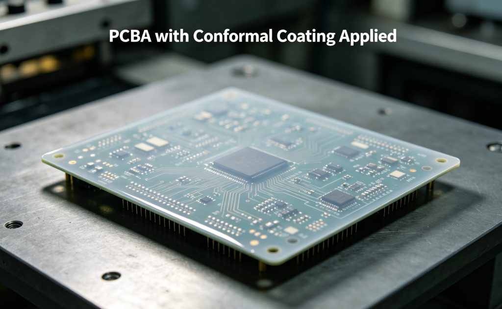
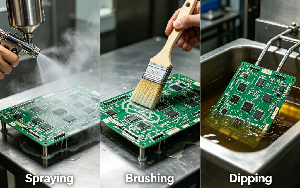
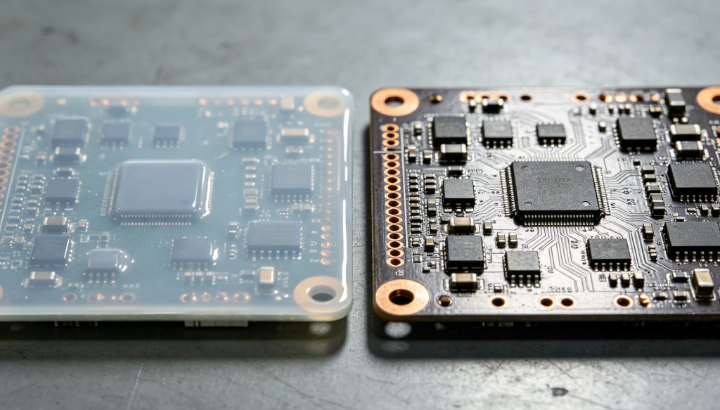
Conformal coating – adds $1–3 per board
Box build / housing – if you want the PCBA put into an enclosure
Shipping – air freight from Asia can double the cost if you need it fast
Customs / duties – sometimes forgotten until the invoice arrives
So How Do You Get a Lower Quote?
Here’s what actually works:
Increase quantity – even from 50 to 200 drops per‑board cost dramatically.
Simplify your BOM – fewer unique part numbers = less setup time.
Use standard parts – no weird voltage resistors or odd‑size connectors.
Ask your CM for alternative sourcing – they often find cheaper genuine parts.
Combine orders – if you have two designs, run them together to share setup.
PCBA Defects That Will Ruin Your Day (And How to Stop Them) You design a board. You send it to the factory. You wait three weeks. The boards arrive.
You plug one in… and nothing happens.
Or worse – it works for five minutes, then a puff of smoke comes out of a tiny capacitor, and you spend the next two days with a multimeter and a microscope, trying to figure out what went wrong.
I’ve been there. Most hardware people have.
The good news is, most PCBA defects follow the same patterns. Once you know what to look for, you can spot them early – or better, stop them from happening at all.
Here are five defects I’ve seen more times than I’d like to count, and what actually causes them.
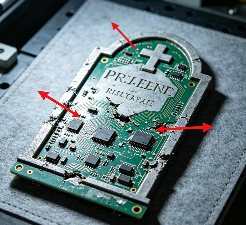
Tombstoning – When a Tiny Part Stands Up Like a Gravestone What it looks like A small capacitor or resistor (usually 0402 or 0201 size) is standing on one end, not soldered flat. One side is attached, the other is pointing up in the air. It looks like a tiny headstone.
What actually happened During reflow, one end of the component heated up and melted its solder before the other end. Surface tension pulled the part upright.
Why it happens
Uneven copper pads under the part – one side connects to a big copper pour (heats slower), the other to a thin trace (heats faster)
Poor solder paste printing – more paste on one side than the other
The part is too small for the pad design
How to avoid it
Make sure both pads have similar thermal mass (add thermal relief spokes if one side connects to a ground plane)
Check your paste stencil design – keep paste volumes balanced
If you’re using 0402 or smaller, ask your CM about their tombstone experience. Some machines handle them fine, some don’t.
Real story A customer once had 30% tombstoning on a batch of 500 boards. They blamed the assembly house. We looked at the layout – one pad had a thermal relief, the other was solid copper. Fixed the design, next batch had zero tombstones. Cost them nothing to fix, but they wasted weeks of troubleshooting.
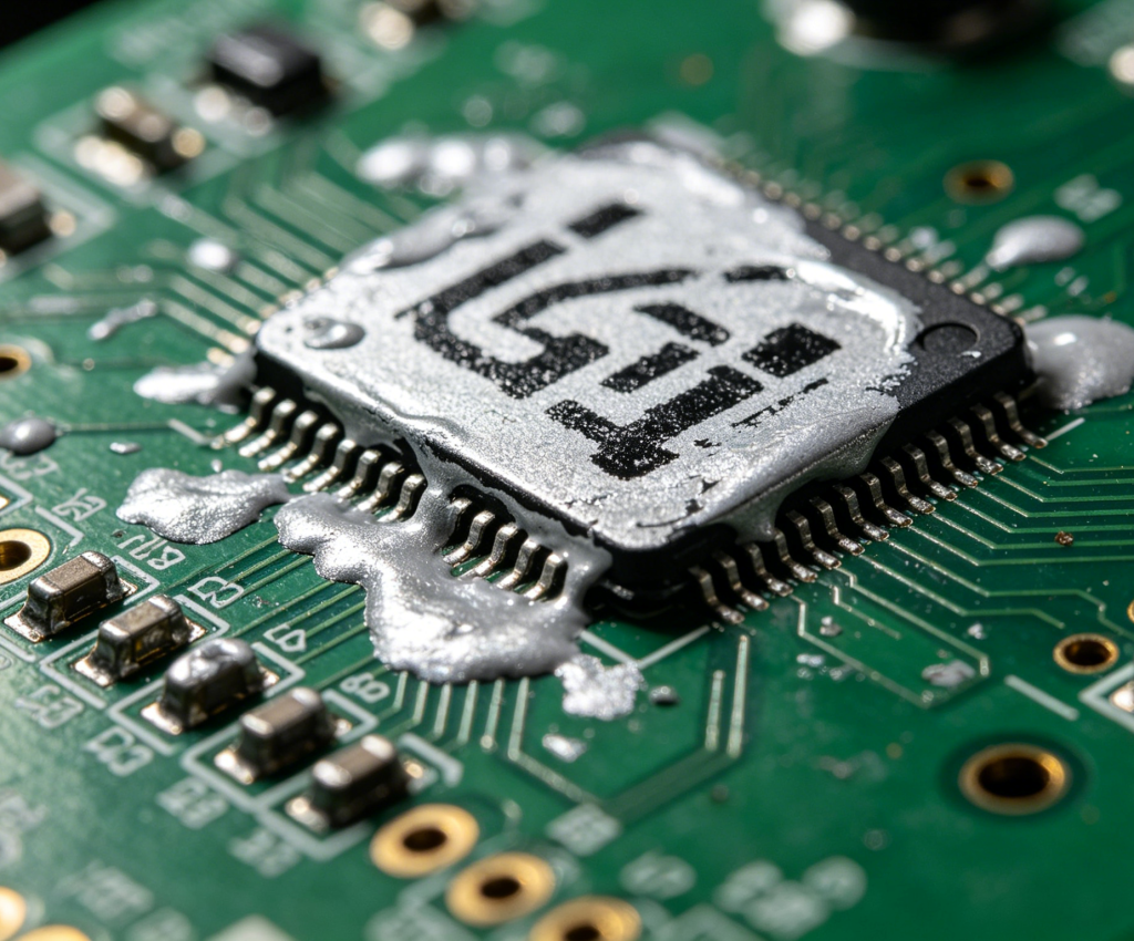
Solder Bridges – When Solder Connects Things That Shouldn’t Touch What it looks like A blob of solder shorts two adjacent pins – usually on fine‑pitch ICs like QFPs or connectors. Sometimes it’s obvious. Sometimes it’s a tiny hair of solder you can only see with a magnifying glass.
What actually happened Too much solder paste deposited between two pins. During reflow, the paste melted and flowed sideways, connecting the pads.
Why it happens
Stencil apertures are too large or too close together
Stencil is too thick for the pin pitch
Solder paste is old or has poor slump resistance (it spreads before reflow)
The pick‑and‑place machine misaligned the part slightly
How to avoid it
Use a thinner stencil for fine‑pitch parts (0.1mm or 0.12mm instead of 0.15mm)
Reduce the aperture size or use “home plate” shaped openings instead of full rectangles
Ask your CM to run a solder paste inspection (SPI) – it catches bridges before reflow
Real story A 0.5mm pitch connector kept bridging on one customer’s board. The assembly house tried everything – different paste, different oven profile. Finally we reduced the stencil aperture width by 15% and the bridges disappeared. Such a small change, but it made all the difference.
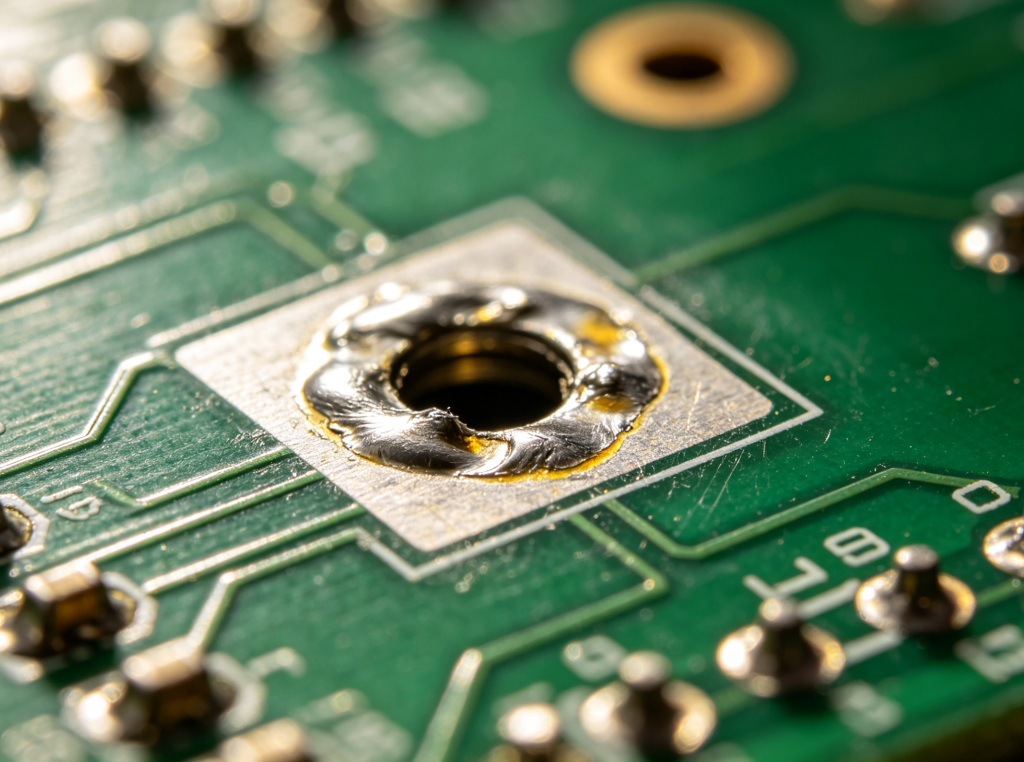
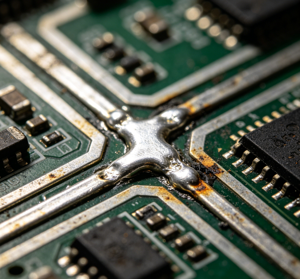
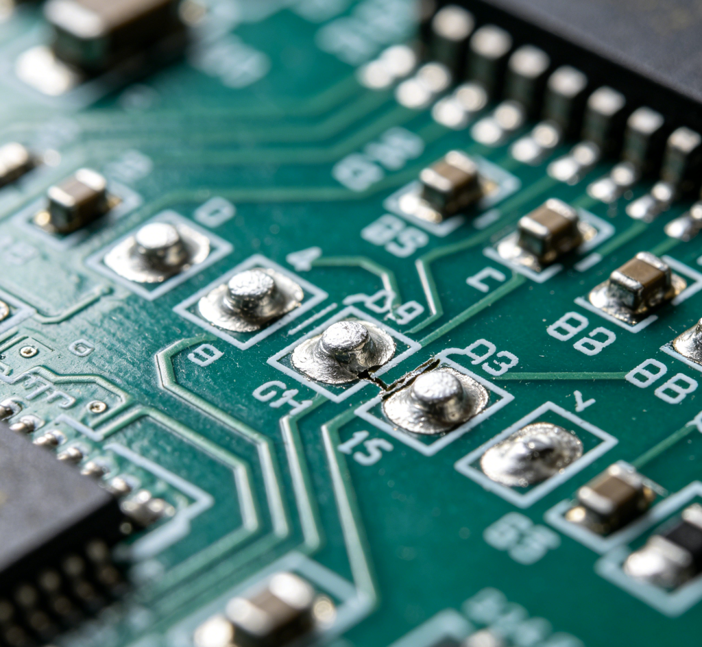
Insufficient Solder – A Weak Joint Waiting to Fail What it looks like The solder doesn’t fully wet the pad or the component lead. You’ll see a dull, grainy surface, or the solder looks like a ball sitting on top of the pad instead of spreading out.
What actually happened Not enough solder paste, or the paste didn’t melt properly.
Why it happens
Stencil is too thin or apertures are too small
Paste was old or dried out
The board surface finish is contaminated (oxidation on ENIG or HASL)
Reflow temperature was too low or too short
How to avoid it
Ask your CM for solder paste thickness data – typical target is 0.1mm to 0.15mm after printing
If using ENIG (gold) finish, make sure the factory stores boards properly before assembly. Gold doesn’t oxidize much, but the nickel underneath can.
For HASL (hot air leveling), be extra careful – the surface can be uneven and cause poor paste release
Why this one scares me Insufficient solder joints often pass electrical test at the factory. They fail later – after thermal cycling, vibration, or just time. A weak joint can work for weeks before it cracks. That’s the worst kind of defect to debug.
Solder Balls – Little Metal Spheres Loose on the Board What it looks like Small, round balls of solder scattered around component legs, usually near passive parts. Sometimes they’re stuck to the board, sometimes they roll around freely.
What actually happened Solder paste splattered during reflow, or excess paste got squeezed out from under the component.
Why it happens
Paste was too wet or had too much flux activity
The stencil was misaligned, causing paste to print outside the pads
The board absorbed moisture before reflow (popcorning effect)
Reflow profile ramped up temperature too fast
Why it’s bad Solder balls can roll around and eventually short two pads or pins. I’ve seen a board fail intermittently because a tiny solder ball got stuck under a connector after shipping. Took days to find.
How to avoid it
Proper reflow profile – slow ramp rate (1‑2°C per second)
Dry the PCB before assembly if it’s been sitting for a while (especially for moisture‑sensitive boards)
Check stencil alignment and cleanliness
Quick test If you see solder balls, ask your CM for their reflow profile. A good profile has a “soak zone” that allows volatiles to evaporate slowly before the solder melts.
Component Shift or Skew – Parts That Look Drunk What it looks like A chip or resistor is rotated slightly on its pads, or it’s sitting off‑center. Sometimes it’s just a few degrees. Sometimes it’s so bad that leads don’t even touch the pads.
What actually happened The component moved between placement and soldering.
Why it happens
Poor board support in the reflow oven – the board warped and the part slid
The pick‑and‑place machine placed it slightly off, and the solder paste didn’t have enough surface tension to pull it straight
Board vibration during reflow (conveyor jitter)
Uneven heating in the oven
How to avoid it
Good fiducial marks on your PCB – essential for accurate placement
Ask your CM about their reflow oven conveyor and board support system
For large or heavy components, consider gluing them before reflow (though most boards don’t need this)
When it’s okay Minor skew is fine if the leads still align with pads. But if leads are off by more than 25% of the pad width, you risk poor soldering or shorts.
Real story I saw a batch where every Bluetooth module was rotated by about 10 degrees. The boards still worked, but the customer rejected them because they looked sloppy. The factory had to rework all 1000 boards at their own cost. The cause? A worn‑out conveyor belt in the oven that shook the boards slightly during heating. Replaced the belt, problem solved.
Bonus: How to Catch These Before It’s Too Late You don’t need to be a factory expert to prevent most defects. Just do these three things before you click “order”:
Get a DFM (Design for Manufacturing) review A good CM will run your Gerber files through software that flags tombstone risks, insufficient annular rings, solder bridge risks, and more. If your factory doesn’t offer DFM, find another.
Ask about their inspection steps Do they have SPI (solder paste inspection)? AOI (automated optical inspection)? X‑ray for BGAs? If they say “we eyeball it,” walk away.
Build a small test batch Even 10 boards can reveal tombstoning, bridges, or alignment issues. Fix the design before you run 10,000.
Final Thoughts Defects happen. Even the best factories have bad days. But most defects are predictable, preventable, and often caused by design choices you can fix for free.
The real cost isn’t the solder balls or the tombstones. It’s the time you spend troubleshooting, the shipments you delay, and the customers you disappoint.
So next time you send a board to assembly, think like the person running the reflow oven. Give them balanced pads, clear fiducials, and a design that doesn’t fight the process.
They’ll thank you. And your boards will actually work.